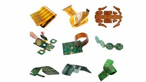
Flexible PCB Boards
As the demand for foldable smartphones increases, flexible printed circuit boards are becoming more popular. Unlike rigid PCBs, they can be folded and bent multiple times without cracking or losing functionality. The main reason for this is that they are made of a polyimide base material, which is tough and can be reshaped without damaging the copper layers inside. In addition, they are also highly tolerant to solder reflow cycles and temperature fluctuations. As a result, they are suitable for use in IoT devices that have curved displays or hinge parts.
IoT devices that monitor human health metrics like heart rate and blood pressure are particularly suited to the flexibility of flex circuits. They can fit comfortably around the wrist or on a necklace to measure vital signs and alert patients when it’s time for medical appointments. Wearable IoT devices are also a key driver for the flexible PCB market. They can be worn discreetly in clothing to monitor physical activity and help people live healthier lifestyles.
For example, fitness trackers are a key application of flexible pcb board because they can be slipped underneath clothing and remain hidden from view while providing accurate readings. IoT devices that monitor environmental factors like humidity and temperature, such as security sensors and industrial robots, also benefit from the flexible nature of these circuits.
Flexible PCB Boards for Foldable Smartphones
While the benefits of flex circuits are clear, it’s important to keep in mind that they are not as durable as rigid PCBs. They are also more expensive, due to extra manufacturing steps and the use of different materials. A webinar by Epec Engineered Technologies on Youtube shows that manufacturing a rigid PCB requires 8 steps, while flex circuits require 17.
When designing a flex circuit, the first step is to select the right type of FR4. There are options available for single layer and multi-layer flex circuits. In addition, it’s important to choose the correct thickness. Choosing too thin a copper trace can increase the resistance to bending, and wide ends at the edge of a flex circuit can be problematic for soldering.
There are also a variety of surface finish types to choose from, including copper oxidation prevention and solderability enhancement. The choice of which to use depends on the design, and a reputable PCB manufacturer will offer these options to their customers.
It’s also essential to decide whether you need a panel plating process or pad-only plating (button plating). With panel plating, the entire circuit board is plated with copper. This method is more stable than button plating, but it may be more difficult to achieve the desired etch yield for small hole patterns. The other option is to use a layer stack that includes both copper and non-copper layers. This allows for greater stability during bending and better signal transmission.